Laser engraved and etched circuit boards!
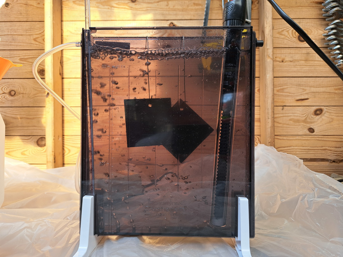
etch tank
Nowadays diode laser engravers are powerful enough to cut through a few millimeters of wood and you can get a fairly large one for under 200 euros.
Cutting wood into shapes always was a makerspace thing I loved to have in my home lab, but it didn't justify buying one.
A laser engraver can also make it easy to prepare bare circuit boards for etching at home though! I'll explain how I do this, and how it makes creating PCB's very easy if you have an etch tank in your lab.
- Concept
- Why roll your own PCB's?
- DIY PCB making comparison
- Required tools
- Required consumables
- Filing/squaring the PCB stock
- Painting the PCB stock
- Prepare the design for engraving
- The copper layers
- The solder mask
- The silk screen
- Drilling holes
- The solderpaste stencil
- The test project
- Time to get creative!
- Related articles
- Presentation May 2025
Concept
Engraving wood and creating wooden boxes is nice. I love even more the idea of being able to create prototype PCB circuit boards at home quickly and easily.
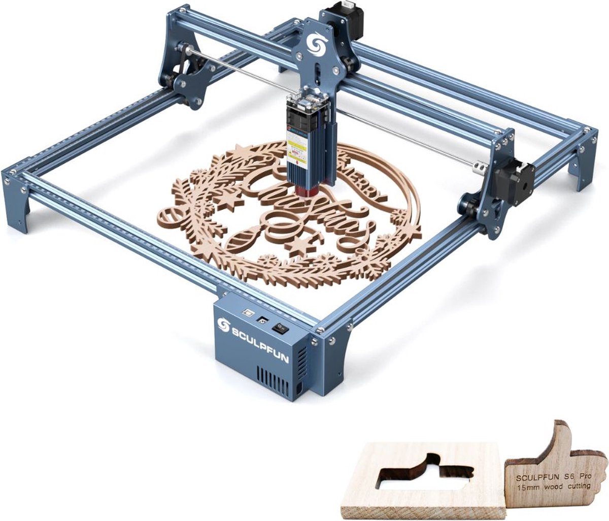
Sculpfun S9 diode laser engraver.
I figured the engraving process can be used to burn away paint to expose it for etching, getting rid of the tedious photo-transfer or toner-transfer masking method which makes alignment for dual sided boards a chore. YouTube showed me several people had the same idea already, and I could learn a lot from them.
Being scared of sharks and lasers, but considering I already had some quality eye protection and a small room where I could set up a webcam to watch the engraving process with, I bought the thing!
One of these youtube videos shows a clever engraving fixture for the circuit board, making it easy to do two-sided boards.
Note
This is still a new project, and on the first attempt I had some issues with engraving accuracy which might be caused by belts not tight enough and the frame not being aligned correctly. I'll update the pictures when I solve these issues.
Why roll your own PCB's?
Nowadays Chinese boardhouses offer cheap prices and fast delivery times. However, it's still several days waiting time, and when you're iterating on a design with a tight deadline and making lots of (beginner) mistakes, this can create a lot of stress.
Next to that, creating your own PCB's adds the artisanal touch to your project.
DIY PCB making comparison
There is always some work involved creating your own circuit boards. I think my method is however relatively convenient compared to other processes.
| Process | Advantages | disadvantages |
|---|---|---|
| Photo transfer |
|
|
| Toner transfer |
|
|
| Fiber laser |
|
|
| Thouters.be method™ |
|
|
Required tools
- A laser engraver. I used a Sculpfun S9, but a CNC3018 with laser addon might be a better option.
- A saw or something else to cut the PCB's with; either a acryl cutting knife, plate shear or fine saw will do
- If you want to do vias or through-hole components
- PCB drills
- some power tool to drill PCB holes with (a hand tool can also work for larger holes)
- If you want to do vias
- A riveting tool (a 4 euro center punch hole marker will work fine)
- An etch tank
- can be as simple as a plastic box/tray with water + iron-3-phosphate
- (you can DIY) a more fancy device
- have it as small as possible to minimize the amount of chemicals, and keep in mind that some chemicals need heating/air bubbling.
Required consumables
- Blank (dual sided) copper clad FR4 board (I used 7cmx5cm PCB blanks from aliexpress, note they measured 71mmx51mm)
- Etch Masking paint: matte black spray paint (I used the cheapest one I could find from the local home improvement store)
- Regular paper painters tape
- Solder Mask paint, either
- industry standard UV curable soldermask paint + a piece of transparency or glass to press onto the paint
- heat resistant (black) spray paint (I used the cheapest one I could find from the local home improvement store)
- Silk screen paint: white UV curable soldermask paint (or acrylic crafts paint, cheap one from a color assortment I had around).
- If you want to do vias
- through-hole 'via rivets' (length 2.5mm, m0.9 500pcs 3eur from Aliexpress)
- To avoid via's
- 1206 size 0Ohm smd resistors to jump across 2 traces
- 0805 size 0Ohm smd resistors to jump across 1 track.
- An etching chemical (I use sodium persulphate from reichelt - needs heating but etches very well)
- optionally: 150T silkscreen printing mesh to spread the UV paint more evenly
Filing/squaring the PCB stock
The boards need to be fairly exact dimension-wise, and also need to have nice right angles. To make it easy to prepare them, I made 3D printed parametric jig to clamp the PCB stock and easily file the pcb to size.
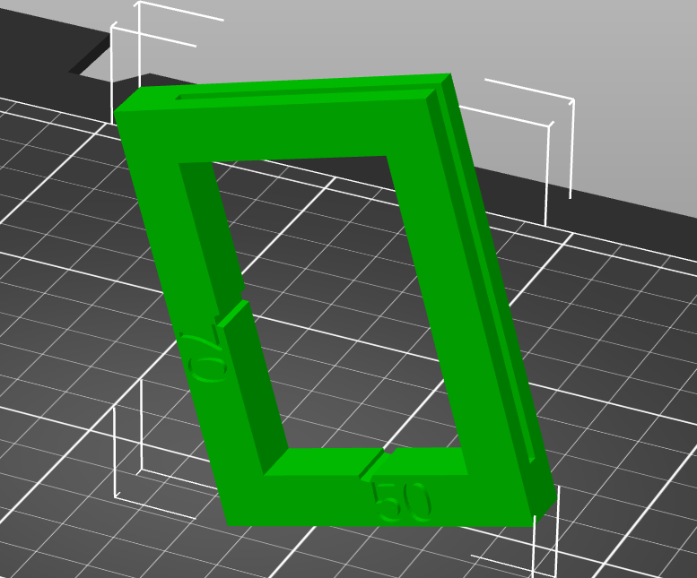
Parametric to-size perpendicular filing jig
You can slide a pcb into this template from two sides, in the middle it has an opening so you can see that the pcb edge is completely against the template.
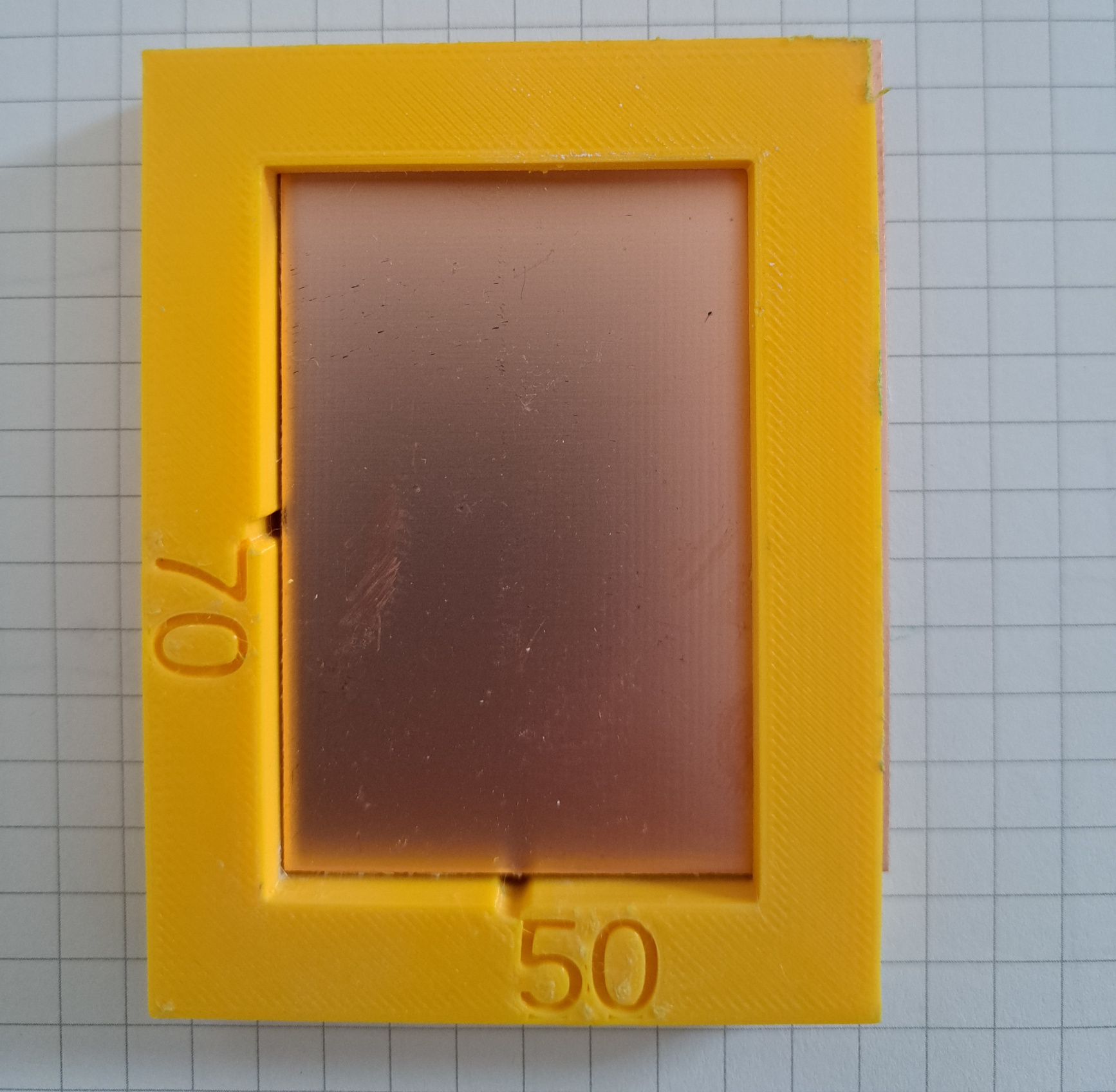
filing jig with pcb inserted
I have one that is 1mm to large, and one of the exact dimensions, the larger one is used to create the first right angle between two adjecent sides, the second exact one will trim the other two sufficiently to perfection.
Use it this way:
- Change the openscad file to have the board dimensions, set the oversize value to 1 (mm). Or, if the bare pcb is very trapezoidal, you may need to file away more than 1mm to get the sides perpendicular and a larger value may be required.
- generate and print the two jigs
- Put the pcbstock in the largest jig and make sure one side of the pcb is perfectly aligned with the inside of the jig
- Clamp the jig and file off the parts sticking out. You now have one 90degree angle on the board.
- rotate the pcb 180 degrees, and put the pcb in the jig that is exactly the target size
- clamp the jig and file off the parts sticking out
- the pcb should now be perpendicular and to size.
Painting the PCB stock
Prepare a piece of cardboard sheet with holes to fit several PCB's in to hold the PCB's when painting. I used the the array feature in lightburn to replicate a rectangle in a grid.
- lightly sand with steel wool, clean with isopropyl alcohol
- place the PCB's in the carboard sheet with holding squares. Put the cardboard in a cardboard box to catch excess paintdrops and to angle the sheet.
- Spraypaint the PCB's on both sides
- let dry, 15min in the sun will do.
Prepare the design for engraving
Design rules
Set the via and drill hole size to something you can drill and rivet.
- minimum clearance: 0.3mm
- minimum track width: 0.8mm
The minimum track with is a bit wider than SMD footprint pads for SOT-23 and SOT-8, but those can be used without issue.
Panellisation
Optionally, you can panellize several boards to etch several designs on one piece of feedstock. To do that:
- Create a new separate kicad project.
- open the board editor and choosing "Append board".
- Group everything in the board (right click selection, group) and select 'create from selection' 'create array'.
Note
The array intervals should include the board size, so measure those first and add some inter-board spacing for sawing later on.
Generate SVG files
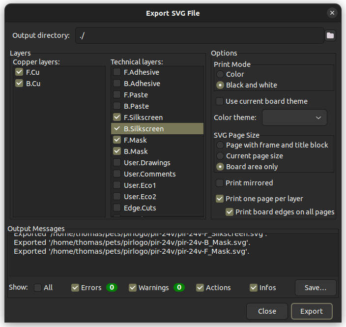
Kicad export settings
Generate bitmaps
I created this bash script I call prepare.sh that uses the ImageMagick 'convert' command line tool to do the boring work of inverting, mirroring and centering the design on the pcb feedstock. Somehow the svg's from KiCAD don't seem to render correctly in LightBurn.
#!/bin/bash
set -ex
echo "$1 board size x (mm)"
echo "$2 board size y (mm)"
echo $3 - input
echo $4 - output
border_cm=0.05
x_mm=$1
y_mm=$2
infile=$3
outfile=$4

echo "$cm - substrate size (rectangle)"
dpi=3000
echo $dpi - dpi
x_pixels=$(python -c "print(int(round($x_mm* 0.1* $dpi / 2.54)))")
y_pixels=$(python -c "print(int(round($y_mm* 0.1* $dpi / 2.54)))")
border_pixels=$(python -c "print(int(round($border_cm* 1.0* $dpi / 2.54)))")
echo pixels: $y_pixels $y_pixels

#render as bitmap
inkscape "$infile" --export-filename="exported.png" -d $dpi
#remove transparency
convert exported.png -format png -background white -alpha background -alpha off nontransparent.png

#invet colors
case $infile in
      (*_Cu*)
        echo image should be inverted
        convert nontransparent.png -channel RGB -negate inverted.png
      ;;
      *)
        #do nothing
        cp nontransparent.png inverted.png
      ;;
esac

convert inverted.png -gravity center -extent ${x_pixels}x${y_pixels} -background white "$outfile"
case $infile in
      (*-B_*)
        echo image should be mirrored
        convert "$outfile" -flop "$outfile"
      ;;
esac

#cleanup
rm exported.png
rm nontransparent.png
rm inverted.png
This wrapper script then calls the previous script for each svg file:
#!/bin/bash
set -ex
for file in *.svg
do
    ./prepare.sh 51 71 $file "${file%%.*}".png
done
Use boardloom to create a Lightburn project
Creating a lightburn project, importing 6 layers and manually drawing the contours cut layer takes a lot of time, and I don't like manual GUI work. Fortunately the LightBurn file format is XML based and very easy to understand. I created a python program I call Boardloom that creates a project file based on a simple configuration file and the KiCAD output.
This allows you to keep your laser settings across projects and save a lot of time. Here is an example of a configuration file:
project:
  input_files_prefix: "pir-24v-"
  output_name: "pir-24v.lbrn2"
board:
  width: 50
  height: 70
  workarea_x: 120
  workarea_y: 110
layers:
  - board_contour:
    handles_dia: 10
    line_settings:
      max_power: 100
      speed_mm_sec: 5
  - match: "F_Cu"
    name: "Copper Front"
    image_settings:
      mirror_y:  true
      max_power: 80
      speed_mm_sec: 10
      dither_mode: "threshold"
      line_interval_mm: 0.0847
  - match: "B_Cu"
    name: "Copper Back"
    hide: true
    image_settings:
      mirror_y:  true
      max_power: 80
      speed_mm_sec: 10
      dither_mode: "threshold"
      line_interval_mm: 0.0847
  - match: "F_Mask"
    name: "Soldermask Front"
    center_on_board: true
    line_settings:
      max_power: 20
      speed_mm_sec: 5
  - match: "B_Mask"
    name: "Soldermask Back"
    hide: true
    center_on_board: true
    line_settings:
      mirror_y: true
      max_power: 20
      speed_mm_sec: 5
  - match: "F_Silkscreen"
    name: "Silkscreen Front"
    hide: true
    image_settings:
      mirror_y:  true
      max_power: 33
      speed_mm_sec: 5
      dither_mode: "threshold"
      line_interval_mm: 0.0847
  - match: "B_Silkscreen"
    name: "Silkscreen Back"
    hide: true
    image_settings:
      mirror_y:  true
      max_power: 33
      speed_mm_sec: 5
      dither_mode: "threshold"
      line_interval_mm: 0.0847
After running boardloom, you can open the file in LightBurn and start lasering right away, the LightBurn UI will look like this:
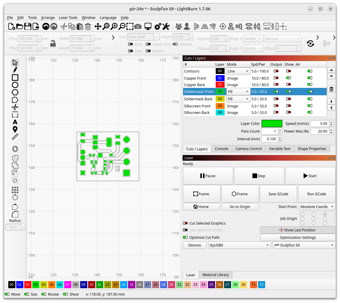
LightBurn screenshot with the PCB project layers.
Manually create a LightBurn project
- Create a contour layer and draw a rectangle the size of the board
- Set the contour coordinates
- Important here is that you do this so that the laser head will move out of place when it is done so you can access the board area easily. I use x=80, y=110.
- Create a handles layer with cutouts to grab under the board to remove it (note the half circles on my cardboard photos).
- Switch to a new layer by clicking the colored layer numbers on the bottom side of the screen
- Drag a png to the application canvas
- In the image/layer settings
- disable bidirectional scanning
- set DPI to 300
- set image mode to threshold
- set speed to 10
- set power to 100%
- you can click set defaults to avoid setting these every time.
- Repeat the steps for the png images for F_Cu and B_Cu (and F_Mask, B_Mask if you will use soldermask)
- Align all layer images by setting the XPos and YPos to be consistent with the contour rectangle
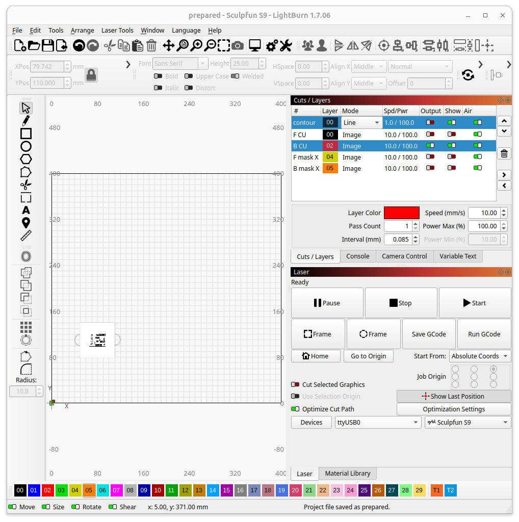
lightburn layers
Prepare the machine for engraving
Warning
- Always use adequate eye protection LASER glasses 👓 when working with LASER machines, or you WILL ruin your eyes, LASERs are not toys!
- Use mechanical ventilation/extraction! Vaporized paint is not healthy!
- Cut a piece of cardboard
- Fix the cardboard on the worksurface, I used these 3d printed pins enlarged in PrusaSlicer at 138% size to hold the cardboard onto my honeycomb bed.
- Laser-cut out the contour of the PCB stock and handle holes out of the cardboard.
The copper layers
Engrave the board's copper layers
- Make sure that in the cuts/layers sidebar, the only output switch is the layer you want to cut/engrave
- engrave side 1
- flip the board
- engrave side 2 (mirrored vertically by the script)
Note that with these settings, the example board of a few square centimeters takes ~20minutes. There is room for experimentation to optimize these settings.
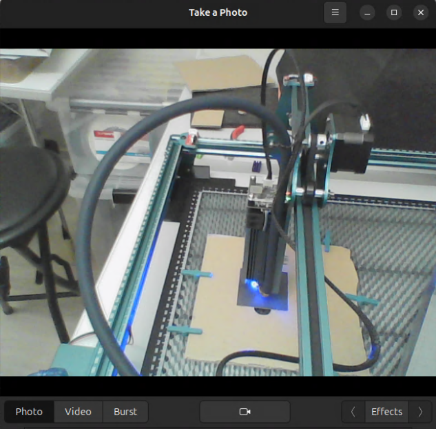
lasering in progress
Etch the board
Warning
Always use adequate eye protection 👓 when working with ACID.
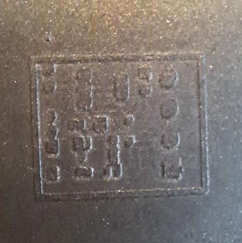
Drill a hole in the board to hang it in the etching tank.
etched front side
etched back side
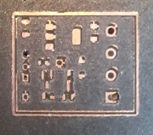
The solder mask
Solder mask protects the copper traces from corrosion and heat.
- Remove all etch mask paint (eg. Wipe the board with isopropyl alcohol)
There are two options here, a simple one that puts paper tape covering over the solderpads and coats the entire board with spraypaint, after drying the tape is removed to expose the pads. In the second option we will coat the entire pcb with UV curable PCB soldermask paint, and clean the paint off the pads with the LASER.
A simple solution for through hole boards
When not doing SMD components, it is possible to use a transparent pcb coating spraypaint like KONTACT CHEMIE PLASTIK 70. This paint can be soldered through, but we can also cover the pads with painters tape before spray painting.
You can also use black heat resistant spraypaint, but you won't see the traces.
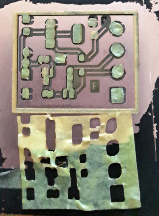
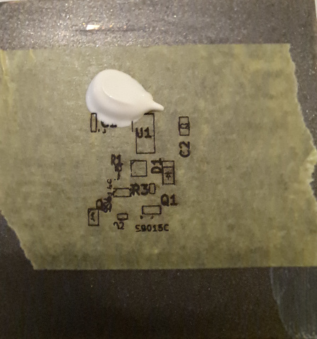
To begin with, cover the necessary board area with painters tape.
board covered with tape (improvised picture with mismatching design files)
We will cut the contours of the copper areas of the solder pads; they need to stay clean of paint.
If not using boardloom;
- Add the soldermask image to the project if not done already, and make sure it is aligned.
- right-click the image and select Trace image.
- Use the 'offset shape' (Alt-O) function to add a 0.5mm clearance around the pad, check the 'delete original shape' box.
- Set settings to 5mm/sec 40% power (white tape) or 20% (yellow tape)
- Laser the image.
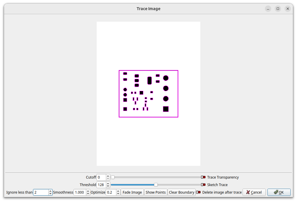
trace dialog
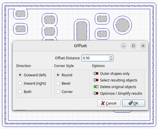
trace dialog
paint mask applied for the soldermask layer
heat resistant spraypaint applied
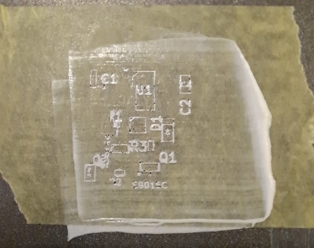
After the spraypaint has dried I use a spudger from a silicone seal kit set to wipe the extending pieces of tape off the board. Any firm but soft plastic (so it does not scratch the paint) can be used for this.
soldermask masking tape removed
You can also use green UV soldermask, in that case I burn the contours of the tape again at 20%,5mm/s before I peel off the tape using tweezers:
First attempt with UV soldermask and acrylic silkscreen paint
Using UV curable paint, laser cleaning pads
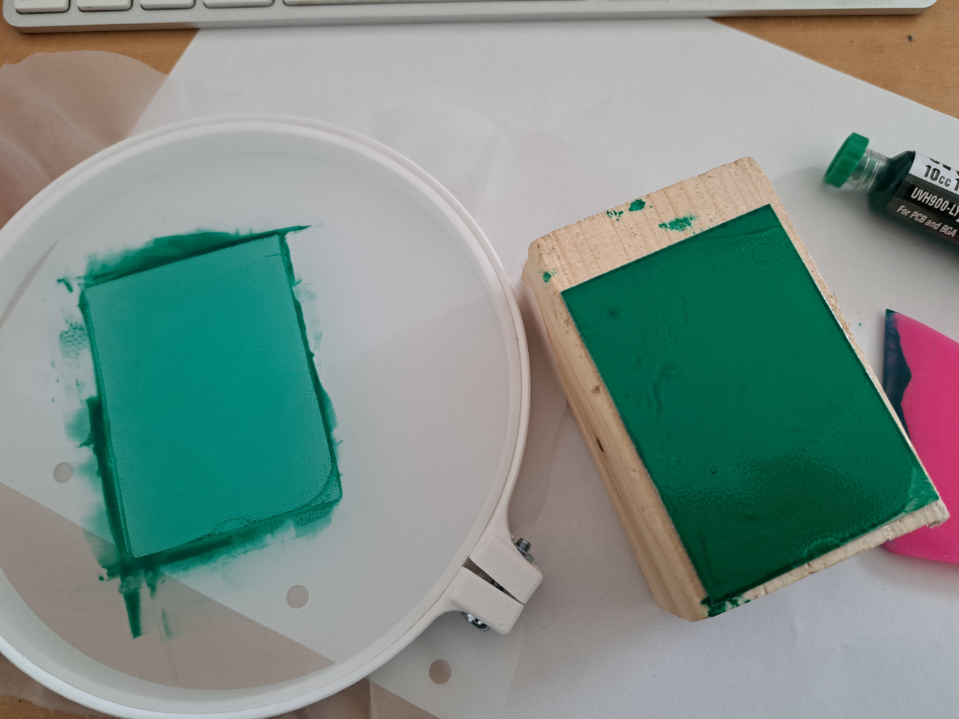
Applying solder mask paint using a 3D printed embroidery ring.
I had some leftover pieces of mosquitto frame extrusions and I quickly modeled a simple corner piece in #openscad so i could build a picture frame sized frame. It seems to do seem to keep an ok-ish tension on the screen printing mesh, better than the embroidery ring does, but I had to add some paper tape to the mesh to make it just as thick as the flyscreen it is designed to work with.
I found a spring loaded pcb holder on the internet, which I figured would go neatly under it, but I ended up designing my own which uses threaded rods cut to lenght, and has magnets to hold the pcb holder down onto to the worksurface.
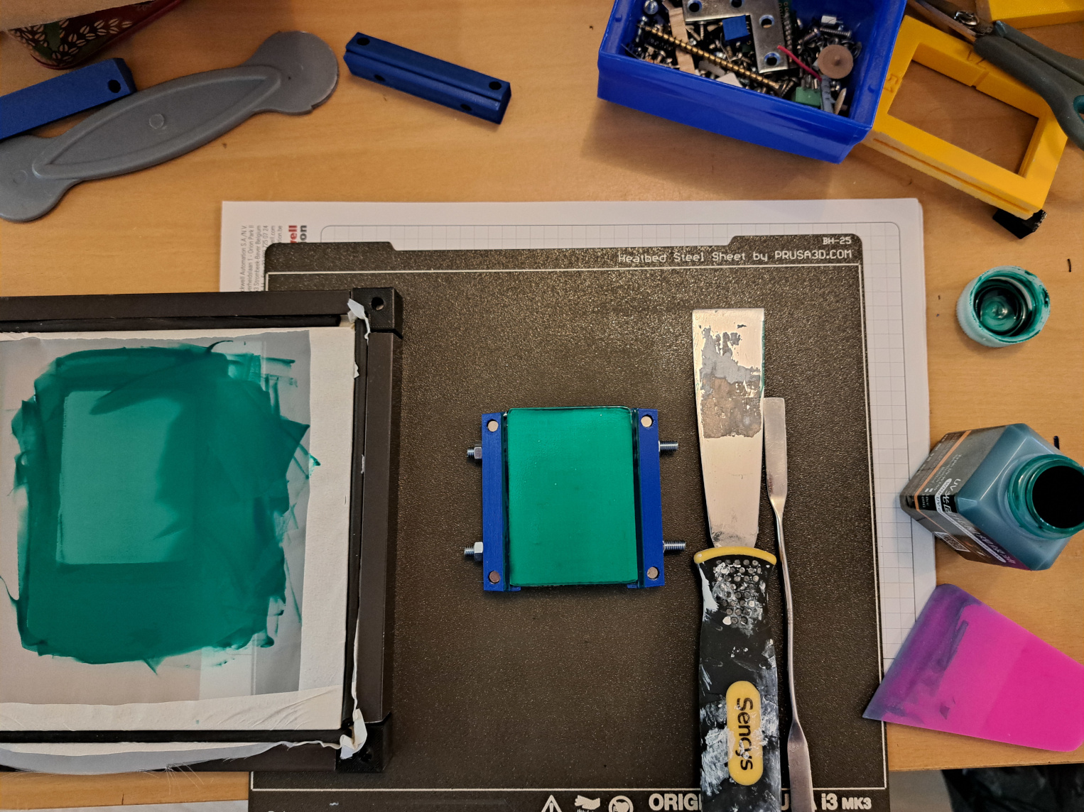
Using the clamp and flyscreen frame
Laser cleaning the pads happens at 5mm/s @ 20%
The silk screen
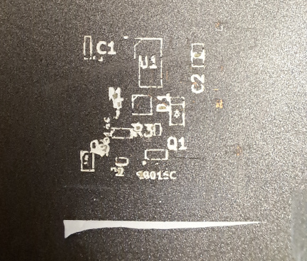
Silkscreen test result
Design rules
For text I used 1.5mm font size, 1.0mm was barely readable. If you want to make sure lines are readable, Use a 0.2mm width. If you use soldermask paint that hides tracks, it's best that you also export the 'Fab' layers which contains outlines of components. However the KICAD footprints overlay the lines on top of pads sometimes. You can try modifying the footprints and removing those if you tweak the footprint to make the lines thicker.
Lightburn design preparation
- Add the silkscreen image to the project
- Double check the design rules enforced that no silk screen got on the solder pads.
- You could also use the 'boolean subtract' function to fix this in lightburn
- right click the image and select Trace image.
- On the Cuts/Layers sidebar, select 'Fill' mode for this layer
- Double-click the layer in the Cuts/layers list to bring up the 'Cut settings editor'
- Set speed to 5 mm/sec
- Set Max Power to 30% (black spraypaint) or 20% (green uv soldermask)
- Disable bi-directional fill
Painting and drying
Apply painters paper tape to the board and engrave the image.
Applying paint
Next we add the acrylic paint, and spread it using a spatula.
Applying paint
I put it on my Prusa 3D printer heatbed at 85 degrees for 15minutes, but I'm not sure what the perfect drying process is.
Note
When using white UV paint, you can apply a coat of uv paint using silk screen printing mesh, dry it on your 3d printer and user your laser to cure the paint (detailed instructions to be determined and added here).
Drilling holes
I already had a Dremel 4200, and 3D printed this drill press fixture from printables.com:
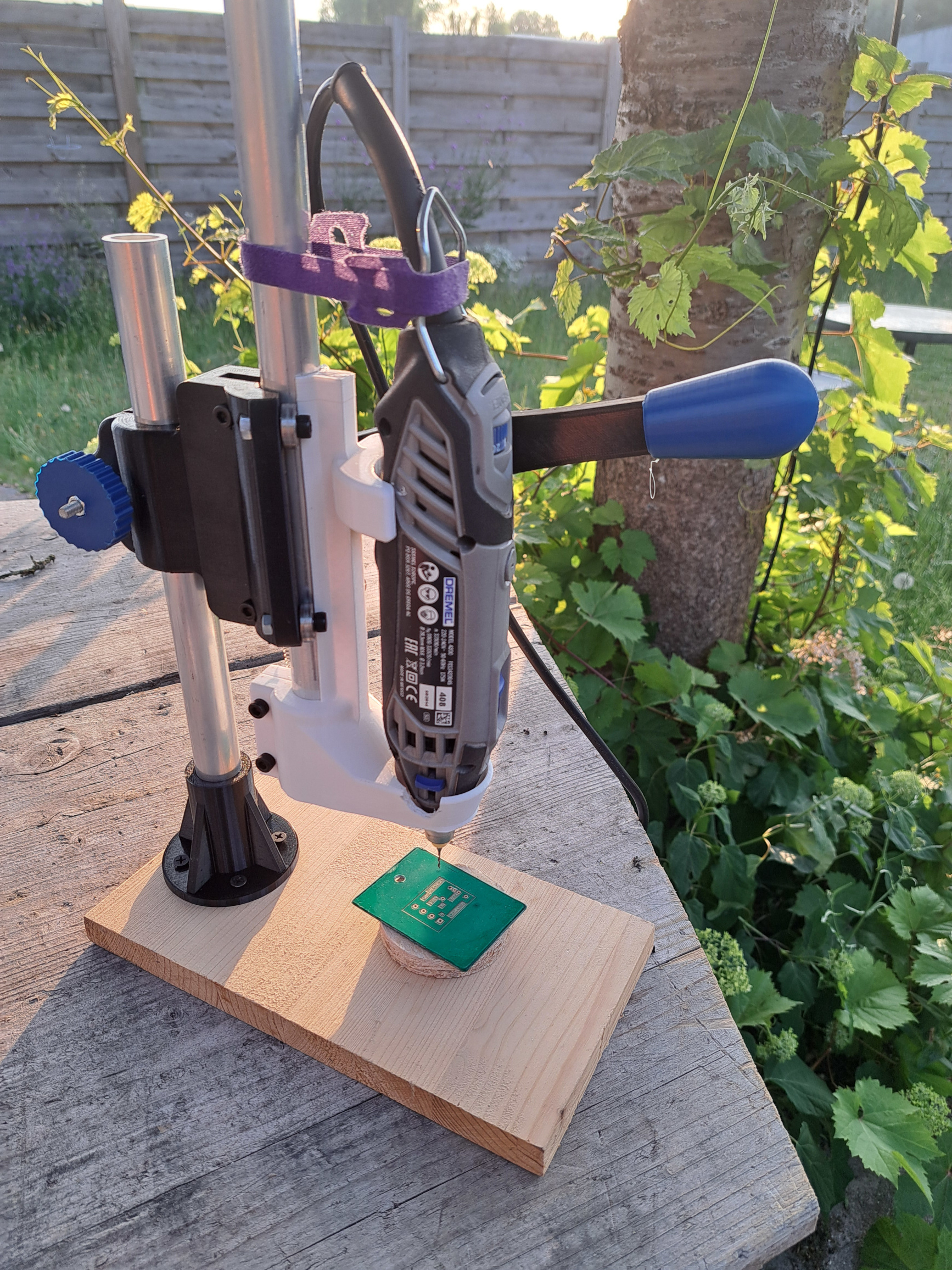
3D printed drill press
I designed a flange to mount the vertical tube on a wooden plank so I could skip the 24+hour print of the base, the flange only took 3hours to print.
The solderpaste stencil
Note
I'm experimenting with doing a solderpaste stencil using the same paper tape method as used for the other non-copper layers, stay tuned!
The test project
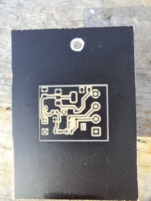
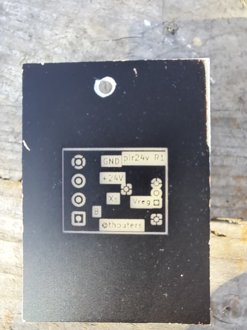
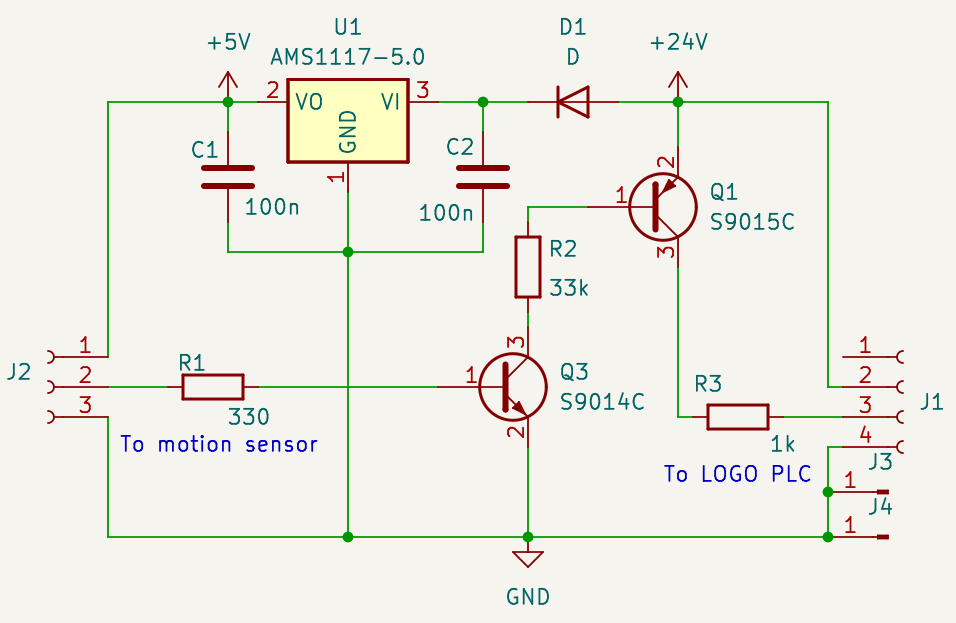
I wanted to try this process out with a small PCB, and already had a simple project in mind. This small circuit drops 24V DC to 5V so a hobby motion sensor (which capacitors are not rated for 24V) can be powered from the house's domotics power supply. The motion sensor outputs a logic high level of 3v3 which needs to be translated to 24V, which is done with a pair of transistors. The motion sensor 2.54mm pin header is included, along with 5.08mm pitch screw terminals. A few via's are put onto the board, although they may not be functionally necessary.
For the via's brass rivets will be used, which i will solder, so i wanted some heat stops around the pads. To save time if this can be set in KICAD, I just added a few 2.54mm pin headers
The png output is shown here:
Simple project to try out the pcb fabbing process
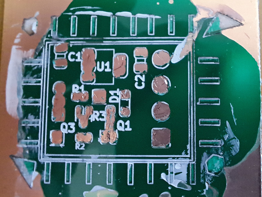
The populated end result
B_Cu
F_Cu
B_MaskCu
F_Mask
Time to get creative!
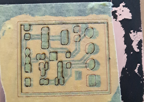
Here is a picture of the second board design I etched, there is a hand drawn part as well, done with permanent marker. DIY etching opens up this possibility!
the morse crab
Presentation May 2025
Thumnail of the talk video
I gave a presentation about this on Newline.gent, which was recorded and can be viewed at: https://www.youtube.com/watch?v=GN7vuh23kpM
You can download the presentation here:
 newline2025-rolling-your-own-pcbs-nohandouts.pdf newline2025-rolling-your-own-pcbs-nohandouts.pdf
|
Liked something? Worked on something similar? Let me know what you think on Mastodon!
You can use your Mastodon account to reply to this post.